-
(b.) - ?1951
Bio/Description
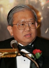
An IBM Fellow and the Vice President of Science and Technology at Thomas J. Watson Research Center, IBM Research Division in Yorktown Heights, New York, his contributions to advanced bipolar technology had a major impact on IBM S/390 mainframe systems. In his capacity, he directs the strategy for computing systems of the future and oversees the research activities in the areas of physical science, advanced semiconductor science and technology, subsystem integration, and advanced communication technology. During the 1980s, he conducted pioneering work on the polysilicon emitter/single crystal silicon interface that led to the world?s first double-poly bipolar technology to manufacturing. The successful commercialization of this technology formed the basis of semiconductor devices that were deployed in the IBM S/390 mainframe computers. More recently, his contributions to CMOS miniaturization and DRAM devices have had a profound impact on IBM?s leadership in CMOS process technology and DRAM manufacturing. Born in Taiwan, China, he received his B.Sc. and M.S. degrees in Physics from National Cheng Kung University, Taiwan in 1974 and 1976, respectively. He then went on to receive his M.S. and Ph.D. Degrees in Electrical Engineering from Yale University in 1979 and 1985, respectively. Having joined IBM in 1984; from February 1999 to February 2003, he was the Director of Advanced Logic/Memory Technology Development at the Semiconductor Research and Development Center, IBM Microelectronics Division in East Fishkill, New York. During the period of 1992 to 1999, he was the Senior Manager responsible for the 64Mb/256Mb/1Gb DRAM Technology Development in IBM/Siemens/Toshiba DRAM Development Alliance. Before assuming his role as the Project Manager in DRAM Development, he held a variety of managerial assignments in his career at IBM, including Functional Manager of High-Performance Technology, Manufacturing Engineering Manager in the Bipolar VLSI Line, and Manager of Optical Lithography Development at Watson Research Center. BiCMOS is an evolved semiconductor technology that integrates two formerly separate semiconductor technologies - those of the bipolar junction transistor and the CMOS transistor - in a single integrated circuit device. He is a strong advocator for international cooperation in technology development and has been a technical leader in several highly successful multinational development programs that have become models for future industrial joint development programs. He has published more than 70 papers in technical journals and conferences, and has been awarded more than 25 patents. He has been recognized with several IBM Technical Innovation Awards and was named IBM Distinguished Engineer in 1996. He was elected as a Fellow of the Institute of Electrical and Electronics Engineers (IEEE) in 1999 for contributions to silicon bipolar and DRAM technology development. Also in 1999, he was named IBM Fellow, the highest honor a scientist, engineer, or programmer at IBM can achieve. In 2005 he was elected Fellow Member of American Physical Society (APS), and in the same year, he was elected to receive the Asian American Engineer of the year Award. In 2011, the Institute of Electrical and Electronics Engineers (IEEE) honored him with the 2011 Ernst Weber Engineering Leadership Recognition award acknowledging his ?exceptional managerial leadership and contributions in the field of silicon chip technologies?.
-
Date of Birth:
1951 -
Noted For:
Major contributor to CMOS miniaturization and DRAM devices which have had a profound impact on IBM’s leadership in CMOS process technology and DRAM manufacturing -
Category of Achievement:
-
More Info:


